
 Process")
Understanding the PCBA process is essential for engineers, designers, and anyone connected to the electronics industry. It serves as the bridge between raw circuit boards and the functional electronic devices that power our modern world.
In this article, we will take a look at the various stages that make up the printed circuit board assembly (PCBA) process and contribute to the creation of reliable electronic products.
Let’s get started!
Step 1: Get a Bare Circuit Board
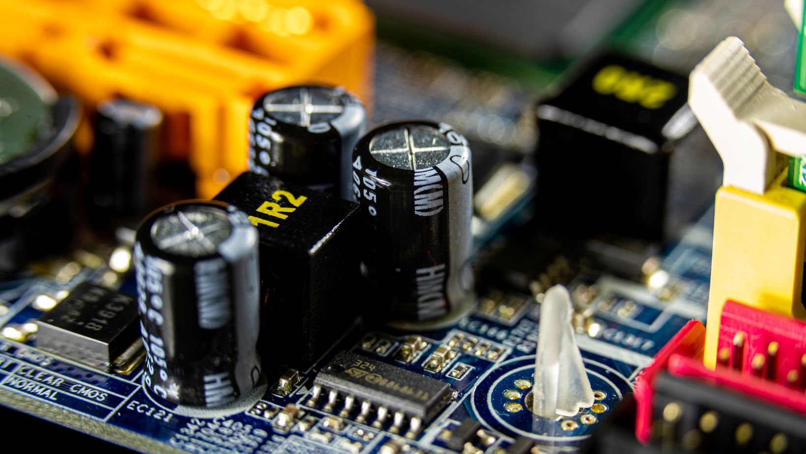
Imagine the bare circuit board as the canvas for our electronic masterpiece. It is a flat, unassuming piece of material – usually made of fiberglass – covered with thin copper traces.
These copper traces are like the highways that guide the flow of electricity. Think of them as the roads on which our electronic components will eventually travel. It’s a clean slate – eagerly awaiting the addition of components that will bring it to life and turn it into a functional electronic device.
Step 2: Place the Components
Now, once we have a bare circuit board available, a team of experts or specialized machines will carefully place tiny electronic components onto it.
It’s a bit like putting together a complex jigsaw puzzle but with utmost precision. Each component – be it a microchip, resistor, capacitor, or diode – has its designated spot and follows a detailed blueprint or design file.
This intricate process ensures that each piece fits perfectly and the circuit board is ready for the next stage, where we’ll lock them in place with a special technique called soldering.
Step 3: Soldering Technique
We use soldering to keep everything in place. It’s like glue, but better!
Solder is basically a low-melting-point metal alloy that transforms into a liquid when heated at low temperatures. Skilled technicians or machines carefully apply this molten solder to the connection points between components and the copper traces.
As it cools and solidifies, it creates strong electrical connections. Common soldering techniques include wave soldering, reflow soldering (used for surface-mount components), and hand soldering (for precision work).
Step 4: Inspection
Quality control is our guardian against imperfections. Highly trained inspectors will usually scrutinize the PCBA assembly for misaligned components, soldering defects, and potential issues.
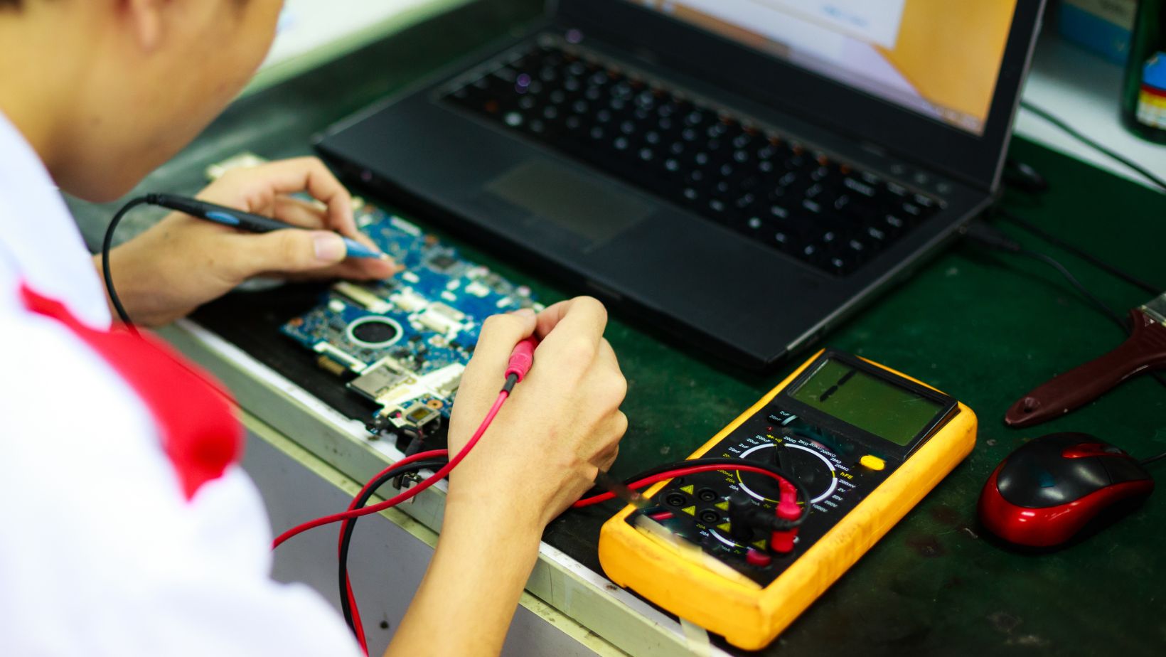
Automated optical inspection (AOI) machines are also used. They are equipped with cameras and advanced algorithms to scan for visual irregularities. Another method is X-ray inspection, which can peek beneath components to ensure hidden connections are flawless.
Step 5: Functional Testing
Now comes the part where the assembled board goes through tests to make sure it works as intended. Think of it as a final exam for your device. If it passes, it’s ready to power up and do its job.
Different tests will be used to check the circuit board’s performance. For example, boundary scan tests will assess interconnections, and in-circuit testing will evaluate individual electrical components.
Environmental testing will subject the device to extreme conditions to ensure it can handle varying climates and stresses. Any anomalies will need adjustments and corrections.

%20Process)